���������ܣ�DSP��Ƶ��ռ���ս��E��
By Doug Morrissey
Vice President and CTO
Octasic, Inc.
For years, Digital Signal Processor (DSP) designers have tackled the daunting task of providing high-performance chips, in a small footprint, with no compromise to the flexibility and software programmability.
As new applications have evolved at a staggeringly high speed, the DSPs provided must match that speed with power, performance and shelf-life endurance to meet today��s challenges and be ready to embrace tomorrow��s applications. These high-performance multi-core DSPs are increasingly used in telecommunications access, edge and infrastructure equipment to process voice, video and radio signals.
Until now, telecommunications equipment manufacturers used dedicated ASICs or DSP-ASIC combinations to achieve their goals. Today, these new DSPs can replace those cumbersome solutions, and if powerful enough, they can provide the flexibility that older solutions cannot. These flexible solutions are a boon for access and infrastructure equipment that must last many years in network deployments. Given the extended service life of these types of devices and applications, the keys to success are flexibility, adaptability and field-programmability.
In today��s technology sphere, ASICs are not as flexible or field-programmable as a DSP, but DSPs can be power hungry, putting gateway designers in a conundrum. But, there��s hope: the new generation of multi-core DSPs can be high-performance and power-efficient. The technology exists to achieve this, but first, the issue of power dissipation, the ��power crisis��, must be overcome.
The Power Crisis
Today��s chips suffer power dissipation from two sources: static phenomena in the form of leakage; and dynamic phenomena in the form of switching operations. This power dissipation is most notable in CMOS technology in the 90nm geometry and below. New generations of DSP design, however, can not only alleviate and circumvent that power crisis, but can actually accelerate processing power in infrastructure, access, and edge equipment while containing power consumption and heat dissipation.
Some of the key metrics that define power consumption within a specific CMOS technology are:
�� Supply voltage
�� Gate switching speed
�� Gate input capacitance
�� Gate power consumption
�� Dynamic energy consumed per MAC operation.
Studies have concluded that power density, or power per unit area, for an equivalent function (e.g. a MAC unit) up to and including 0.13��m geometry, is fairly stable. However at 90nm this parameter suddenly rises.
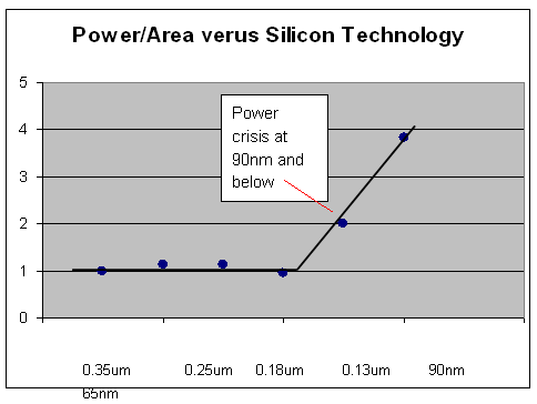
Until achieving 0.13��m technology, DSP designs would benefit from both an increase in performance and a reduction in power, which allowed more circuits to be packed onto a single die. This resulted mainly from the reduction in geometry coupled with a reduction in voltage. Once the technology hit 90 nm, all bets were off.
It��s now a matter of trading performance for functionality, an equipment manufacturer��s nightmare: more circuits in a single package with lower performance; or fewer circuits with less functionality.
As the ��power crisis�� continues, designers have been increasing power consumption to achieve benefits in both performance and functionality. But a new risk occurs: heat dissipation limits have been reached and the resulting problems can already be documented with the latest generation of generic multi-core DSPs on the market today.
Zero-Sum Game: Static Power-Performance
Because performance is the main goal in infrastructure, access and edge applications, zero standby power is usually not a concern for designers. As a result, a general-purpose silicon process has been the preferred approach to optimize performance, rather than a low-leakage silicon option. Choosing low-leakage silicon would provide lower standby power, but also lower speed and performance.
This requires a choice of transistors.
In battery-operated devices, High-Voltage Threshold (HVT) would be optimal, but in infrastructure applications, a Standard-Voltage Threshold (SVT) technology is preferred.
Take, for example, a design using HVT logic operating with a supply voltage of 1.2V, which continually draws 20mW of leakage power. While operating at maximum capacity, it consumes 1W of dynamic power.
An identical design using SVT logic operating at 1.0V delivers roughly the same performance and draws 5 times more leakage power (100mW), but dynamically consumes only 694mW (1.02 /1.22 = 0.694).
The higher-leakage SVT design will therefore only consume a total of 790mW of power compared to 1.02W for the HVT design. That is a 23% power savings.
Comparison of Power Consumption of HVT and SVT Designs
|
Power Consumption |
HVT design (VDD = 1.2V) |
SVT design (VDD = 1.0V) |
|
Leakage Power |
0.02W |
0.10W |
|
Dynamic Power |
1W |
0.69W |
|
Total Power |
1.02W |
0.79W |
|
Performance |
Both designs deliver the same performance. | |
Although it is counter-intuitive, this example illustrates that the use of higher-leakage SVT logic versus low-leakage HVT logic can save power overall, due to the high amount of switching activity in the circuit. This is particularly useful for Multiply-and-Accumulate (MAC) circuits but is counterproductive when used on circuits with low activity factors like RAMs and test circuits. As a result, SVT logic is the way to go for infrastructure, ��always-on�� equipment.
Being Dynamic: Power-Performance Optimization
Both clock trees and logic transitions cause dynamic power consumption, and must be dealt with in the new generation of multi-core DSPs. Power-performance metrics can be substantially improved by aggressively optimizing the design of these two power culprits.
Clock trees (the network of wires and buffers used to deliver a synchronous clock to flip-flops of a design) suck some energy from a chip during the flip-flop operation itself. Power is also expended in charging and discharging the often massive clock trees that span modern high speed chi
����Ķ�:
- ...2008/10/27 11:14��DSP��ƣ����������ܵ��ռ���ս
- ...��ͼ����������DZ��屳��ij��漶��ȫ���Ҫ��
- ...��ʹ���а�ȫ���ϵ�����洢������ȫ������ϵͳ
- ...������ƫ�ò�����Դ������Ľ��½�չ��Ӧ��
- ...�����¿�˹����ijƷ�����ܲ���������������ƪ
- ...�����ߵ���ʽ�¶ȼ��������ϵͳ�����ŵ���ʧ���Ӱ��(��)
- ...�����ߵ���ʽ�¶ȼ��������ϵͳ�����ŵ���ʧ���Ӱ��
- ...��RTD����ϵͳ�����ŵ���ʧ���Ӱ��
- ...������BR/EDR �� Bluetooth Smart��ʮ����Ҫ����
- ...�� ��о���������Уδ�������˻�������ƴ���������ʽ����
- ...�� ̽�صڶ�������ɽӥ�����¡����������鼼����̳��
- ...�� ��2018�й��뵼����̬����ᡱ�ڽ���ʡ��������
- ...�� �������¹滮��CITE 2019�t���ǻ�δ��
- ...�� ��������������TI���ײ������������ڴ�������ܵ�����
- ...�� �ⷨ�뵼�壨ST����Cinemo��Valens��CES 2018չ��������ʾ������Ϣ���ֽ������
- ...�� �������ɵ�·��ҵ���·�չ�߷���̳�����ھ��ٿ�
- ...�� ������ǿ�Ƴ���PCIM����2017չ
- ...�� GPGPU����������й�оƬ��ҵ�Ŀհش�
- ...�� ��������Ʒ�����Wi-Fi���ӵ��ĸ��ؼ�����
- ...�� �������й�MEMS���ܴ�������ҵ��չ��ἴ���ڰ��������Ļ
- ...�� IAICר��������й�о��Ӧ�ô��£���Ϣ��ȫ�߷���̳��������
- ...�� ���ܿ�����Դǯλ����
- ...�� ���5G���ײ�OTA ���Լ���
- ...�� ����г����������ƶ�Molex��ǿ��������ķ�չ
- ...�� �й���ɫ�������˳�������ٿ��ڼ� ����ѧ���ù�̽��ɫ��չ��ģʽ
- ...�� Efinix® ȫ������AI��Ե���㣬�ɹ��Ƴ�Trion™ T20 FPGA��Ʒ, ͬʱ����Ʒ��չ����ʮ������Ԫ��T200 FPGA
- ...�� Ӣ������������ᣬ�����ǻ�������
- ...�� �����Ʒ�������������ֻᱱ������Դר���ɹ�����
- ...�� Manz���ǿƼ�����뵼������ Ϊ��弶�ȳ��ͷ�װ�ṩ��ѧʪ�Ƴ̡�Ϳ��������Ӧ�õ������豸�������
- ...�� �е���BITRODE������ز���ϵͳ˳��������������Դ
- ...�� �е���FTFϵ�е�ز���ϵͳ�б걱������Դ�����ɷ�����˾
- ...�� �е����ʸ�ѹ��Դ����ʽ����ϵͳ�ɹ������е���è
- ...�� �е������ڵ綯�������ؼ������������ֻ��������Ƚ���������